Industry News
Understand in one article, the relationship between the Internet of Things and PCB circuit boards!

01
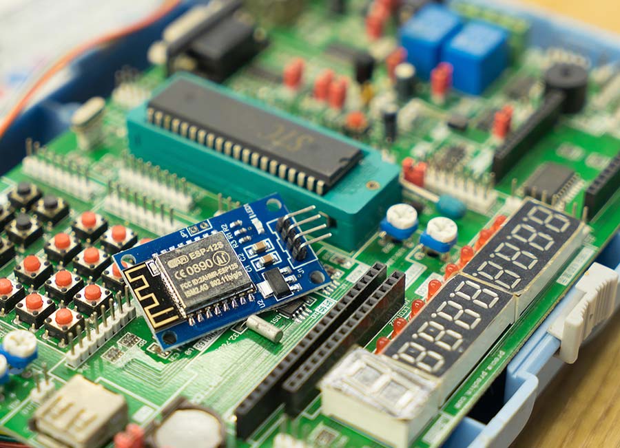
IoT PCB design field
IoT products usually collect information from the real world, hide it in the digital world, and then transmit the data to the cloud. Some analysis will be done and the results will be sent back. Therefore, there are four main IoT design areas:
(A) Simulation
(B) Number
(C) MEMS
(D) Radio frequency
To reiterate the previous paragraph, the MEMS sensor collects data, performs analog-to-digital conversion for input to the microcontroller, and the result is transmitted through standards such as WiFi, Bluetooth and 3G/4G. Depending on the response as part of the device function, reverse path digital-to-analog conversion is also possible.
02
The form and suitability of IoT PCB
Wearable devices illustrate the form challenges faced by many IoT PCB designs. A company that develops smart watches wants its size and weight to be the same as traditional "dumb" timepieces. Internet of Things innovators usually solve this problem from two starting points:
(A) Determine the potential function, and then the developer explores whether it can be placed in a suitable marketable enclosure.
(B) Developers see an opportunity to add a function to an existing product, and then explore whether the function can be completed with the least possible impact on the original product. Either way, complex functions may need to be adapted to the narrow living space.
03
IoT design components
The main impact on "shape and fit" is to correctly identify the components to be filled with the PCB. However, these parts are only required for operation. Your design may require fingerprint readers, different types of MEMS sensors, or different RF standards. You need to lock them as early as possible-and don't forget the external interfaces (buttons, switches, charging ports, etc.).
04
Capture the IoT PCB design intent in the schematic
You have a component type. Now you must determine how to put them together and assign the correct part numbers for the specifications and target dollar cost. The development schematic starts to show you how to achieve it. In addition, the right tools will allow you to perform analog/mixed-signal circuit analysis and identify some signal integrity challenges that you may encounter before proceeding to the actual layout.
05
Simulation, verification, power supply and memory in PCB design of IoT
The IoT design looks simple in terms of function, but it turns out to be more difficult to implement than that. The old adage is that you should catch as many problems as possible early in the process. Consider only the following three challenges (there are more challenges):
(A) The IoT design is small and must often provide long battery life. Therefore, they may need to run in various power states and perform different tasks. Each must be functionally verified.
(B) Similarly, what about the risk of failure due to voltage loss on critical networks? Are certain areas on the board prone to excessive current density? Again, catch these issues as early as possible.
(C) The connection between the microcontroller and the memory is also troublesome and is affected by many factors, including transmission line loss, crosstalk and timing delay. Precisely restricting these connections before layout will reduce future debugging time, especially when using the DDR standard.
06
IoT PCB layout
If you have followed the principles listed, it should be much easier. The outline of the board will now enter the layout, and it should also be known by the two-way cross-probing between the layout tool and the schematic. But there are other considerations:
(A) Component placement. Considering the possible size constraints, layout tools that allow you to switch between 2D and 3D views are particularly useful for IoT design.
(B) Constraint management. Being able to propagate predefined electrical constraints in the process will help you control network categories and groups, and define pin equivalence. If you can use layering rules in the tool, the results will be better.
(C) 2D/3D layout. This function is not just about dropping components. Is the overall structure correct? Can you import the suggested mechanical enclosure and check it against the specifications? The ability to switch views will be of great help in these and other areas.
(D) Rigid-flex board. As mentioned earlier, the rigid-flex board is particularly useful for IoT design only if your layout tool allows you to correctly check its curvature, the position of the part on its layer, its wiring and flat shape filling. If so, you can adopt this rigid-flex design and export it as a solid model to the MCAD system, which can greatly reduce the potential manufacturability and assembly problems of the production line.
(E) Test the IoT design. A good DFT always pays off. For the Internet of Things, it is particularly suitable for metrics such as radio frequency range, battery life, interoperability, and response time. Also check possible operation in a wide temperature range and in multiple power states.
07
Manufacturing and assembly of IoT PCB design
Issues such as resist fragments and copper exposure. Precautions for panelization and the use of database standards can make the design files more smoothly transmitted to the manufacturer, which should also be part of your design process. IoT design usually must work within a very small profit margin to achieve profitability. Any kind of delay or re-rotation will make such items red.